
2022-9-22 8:04:47
Introduction of Pogo pin SMT soldering process
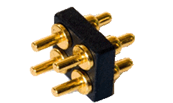
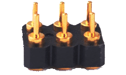
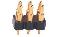
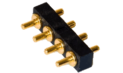
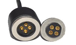
In order to be suitable for large-scale SMT process of Pogo PIN, we generally wrap Tape&Reel for Pogo PIN, mainly for the convenience of SMT machine and over wave soldering.
Electronics factory DIP wave soldering machine, wave soldering) is mainly used for traditional THT hole instrumentation PCB and Pogo pin electric welding process, as well as surface mount and conventional process of instrumentation components, wave soldering its high temperature liquid tin maintain a slope, and formed by special equipment make the liquid tin road similar wave phenomenon, so called "wave soldering"; Surface assembly components suitable for wave soldering processes include rectangular and cylindrical chip elements, SOT, and smaller SOP devices.
Working principle of DIP wave soldering machine:
The wave soldering machine used in the DIP and SMT red glue process in the electronics factory is generally a double wave soldering machine or electromagnetic pump wave soldering machine.
The following takes the process flow of double Pogo pin wave soldering machine as an example to illustrate the working principle of wave soldering:
DIP plug-in welding development and advantages:

DIP plug-in wave soldering machine working principle flowchart:

With the mass production of electronic products, manual use of soldering iron tools point by point solder joints on PCB and Pogo pin board method, can no longer meet the market requirements, production efficiency and product quality. Then gradually invented the semi-automatic/automatic welding group (Mass Soldering) equipment and automatic welding machine. Automatic welding machine first appeared in Japan, as the main production equipment of black and white/color TV sets. Since the introduction of the 1980s, there have been dip welding machine, single wave soldering machine. In the middle of 1980s, SMT technology developed rapidly, and double wave soldering machine appeared.
Wave soldering refers to the soft soldering material will melt tin alloy (lead), electric pump or electromagnetic pump flow into the design requirements of solder wave, can be formed by the injection of nitrogen to solder pool, make the PCB and Pogo pin with components in advance through the solder wave, components and PCB and Pogo pin solder welding end or pin of the mechanical and electrical connection between soft soldering. There are many kinds of wave soldering systems, depending on the geometry of the wave used by the machine.
Compared with manual welding technology, automatic flow welding technology obviously has the following advantages: save energy, save manpower, improve efficiency, reduce costs, improve the appearance quality and reliability, overcome the human factors, can complete manual work can not be completed.
Commonly used DIP crest welding process: insert the component into the corresponding component hole → pre-coating flux → preheating → over crest soldering furnace → cooling → removal of excess plug-in foot → AOI detection.
A thin layer of flux is uniformly applied to the pads on the lower surface of the PCB and Pogo pin, the ends of all components, and the pin surfaces of the PCB and Pogo pin that has finished dispensing (or printing), attaching, gluing, curing, and installing through-hole components, as the PCB and Pogo pin runs forward along the conveyor belt from the inlet end of the wave welder through the flux foaming (or spray) groove.
The action principle of flux:
The reason why molten solder can assume the welding effect is that the metal atoms are close to each other after diffusion, dissolution, infiltration and other effects of the result. At this time, the barrier between atomic interaction is the metal surface of the oxide film and pollutants, is also the most harmful substances to prevent infiltration.
Therefore, on the one hand, measures should be taken to prevent the production of oxides on the metal surface, and on the other hand, various measures and treatment methods should be taken to remove pollution. However, it is difficult to completely avoid these oxidation and contamination in various front-end processes of PCB and Pogo pinA production, even in the process of component production. Therefore, some means must be taken to remove the oxide film and contamination before welding operation. The use of flux to remove oxide film has the characteristics of no damage to the base material and high efficiency, so it can be widely used in the process of PCB and Pogo pinA.
With the completion of the flux spraying process, the PCB and Pogo pin board is transferred into the preheating area through the titanium claws of the wave peak, the solvent in the flux is volatilized, the rosin and active agent in the flux begin to decompose and activate, and the oxide film and other pollutants on the surface of the pad, the end of the components and the pin are removed. At the same time, the printed board and components are fully warmed up.
The PCB and Pogo pin circuit continues to run forward, with the underside of the PCB and Pogo pin first passing through the first wave of molten solder. The first solder wave is a turbulent wave (vibrational or turbulent wave) that hits all pads, component welds and pins on the bottom of the PCB and Pogo pin; The molten solder infiltrates and diffuses on the flux-purified metal surface. The bottom surface of the PCB and Pogo pin then passes through a second wave of molten solder, a smooth wave that separates the bridge between the pins and the solder ends and removes weld defects such as pull tips (icicles).
Wave welding with the enhancement of people's awareness of environmental protection has a new welding technology. In the past, tin-lead alloy was used, but lead is a heavy metal that is very harmful to human body. So now you have lead-free processes. It uses * tin, silver, copper alloy * and special flux and the welding temperature is required to be higher higher preheating temperature. Also, a cooling station should be set up after the PCB and Pogo pin board passes through the welding area.
Traditional tin-lead solder has been used in electronic assembly for nearly a century. Eutectic solder conductivity, stability, corrosion resistance, tensile and fatigue resistance, mechanical strength, technology is very excellent, and the resources are rich, cheap. It is an ideal material for electronic welding. But because lead pollutes human living environment. According to statistics, the amount of lead in groundwater in some areas has exceeded the limit by 30 times. Because Pb is a toxic metal, harmful to human health and very destructive to the natural environment, lead-free welding wire was introduced.
The article comes from : https://www.pogo-pins.com/
