
2026-10-25 11:30:22
How to Solutions to Pogo Pin Heating During Charging
Core principle: Heat generation follows P=I²R. Prioritize reducing contact resistance and current shunting, then optimize PCB heat dissipation, mechanical matching and current control, and finally carry out maintenance.
Troubleshooting sequence for Pogo pin samples or mass-produced products with overheating: First check for poor contact, improper compression or foreign matter; then modify structure and selection; finally adjust PCB and circuits.
I. Pogo Pin Quick Troubleshooting (For overheating samples / mass production units)
1. Measure contact resistance (4-wire method)
For charging pins, stable contact resistance should ideally be <30 mΩ. If it exceeds 50 mΩ, it is usually the main heat source. Measure voltage drop under load instead of only checking continuity.
2. Check compression stroke (most common pitfall)
Recommended working compression: 50%~70% of total stroke.
Insufficient compression → insufficient contact force, sharp rise in contact resistance;
Over-compression → spring fatigue, reduced spring force, pin sticking and heating.
Recommended spring force for charging pins: 80–120 gf. Too low force causes unstable contact; excessive force leads to heavy wear and high overall mating force.
3. Check alignment, foreign contaminants and wear
Offset magnetic mating / male-female housing, one-sided contact, or unsynchronized engagement of multiple pins will cause overheating due to overload on individual pins.
Dust, oil stains and oxide layers, or worn plating will create local hot spots. Clean pin tips and mating pads with anhydrous alcohol.
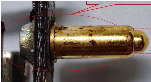
Spring fatigue or worn plating exposing base metal causes progressive heating over service life; replace the pogo pin assembly directly.
4. Rule out bottlenecks in downstream circuits
Small gauge wires, undersized pads, cold solder joints and thin PCB copper foil often cause heat. The heat conducted to the pin may not originate from the pogo pin itself.
II. Pogo Pin Selection & Structural Optimization (Fundamental solutions for new projects)
1. Choose low-resistance constructions; avoid standard straight plunger types where current passes through the spring
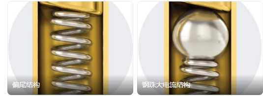
Bias design: The plunger tail is chamfered. When compressed, the plunger presses tightly against the barrel wall. Current flows through the barrel instead of the spring. Contact resistance stabilizes at 10–20 mΩ, suitable for 5–8 A continuous charging.
- Ball structure: A conductive steel ball sits between the plunger and spring. Preferred for high-current applications, rated 10–30 A, low resistance and vibration-resistant, with higher cost.
Standard straight plunger: Current travels through the spring. The spring itself heats severely under high current, not recommended for continuous current above 3 A.
2. Base material and plating
Barrel & plunger: C17200 beryllium copper is preferred for better conductivity and fatigue resistance than brass. Use heat-treated beryllium copper springs to maintain stable spring force at high temperatures.
Plating: Nickel underlayer ≥3 μm + hard gold ≥1.5 μm (≥2.0 μm for high current / long cycle life). Thin gold plating wears through easily and oxidizes, raising resistance rapidly with use.
Mating surfaces must also be gold or palladium plated. A gold-plated pogo pin paired with bare copper on the mating side will still overheat.
3. Parallel pins for current shunting (cost-effective solution)
Joule heat is proportional to the square of current. If one pin overheats at 5 A, splitting into two parallel pins carrying 2.5 A each theoretically reduces heat to 1/4.
Requirement for parallel layout: Tight tolerance on pin length and uniform compression, plus symmetric routing. Otherwise, uneven current distribution will overload individual pins.
4. Larger contact area at pin tip
Use round, large-diameter tips instead of sharp points. Sharp tips create tiny contact spots with extremely high current density, prone to local hotspots.
III. PCB & Pad Thermal Design (Easily overlooked)
1. Enlarge pads: Pad diameter ≥ 1.5 × pin diameter.
2. Copper weight: 2 oz / 3 oz copper for high-current charging PCBs; avoid 1 oz thin copper.
3. Thermal vias: Array thermal vias under pads to conduct heat to inner copper planes / ground planes.
4. Widen and shorten power traces; avoid narrow bottleneck sections.
5. Increase pitch between pins in an array to prevent heat accumulation and reserve convection space.
IV. Circuit & Charging Strategy Control
1. Derate continuous current with sufficient margin: Do not run continuously at the pin’s maximum rated current. Rated current is tested under ideal conditions; derate for enclosed housings.
2. Add current limiting and soft start on the charging IC to suppress inrush current, arcing and heat during mating.
3. Add NTC temperature sensing in sealed assemblies to automatically reduce power or trigger current limit when overtemperature is detected.
V. Mechanical & System-level Thermal Management
Do not fully seal the enclosure; reserve minor airflow channels.
For concentrated heat areas, use thermal silicone gel or thermal pads to transfer heat from pads to the metal housing.
Reliable magnetic positioning ensures centered engagement every time and synchronized contact of all pins, preventing offset loading.
VI. Maintenance Guidelines (End-user side)
Periodically clean pin tips and mating metal surfaces with lint-free cloth and anhydrous alcohol to remove sweat and dust.
Conductive grease is NOT recommended for most charging scenarios; it traps dust and accelerates aging.
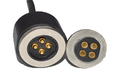
Replace the pogo pin magnetic connector assembly if there is wobble during mating, stuck retracted pins, or intermittent charging.
Quick Selection Reference
<2 A: Standard bias-type pogo pin, gold plating ≥0.8 μm
2–6 A: Beryllium copper bias design, gold plating ≥1.5 μm; prefer dual parallel pins
>6 A continuous charging: Ball-type high-current pogo pin, paired with heavy copper PCB and thermal vias

